


100G 10km QSFP28 LR4 Optical Transceiver
Product Description
Single-mode,100G,10Km,LC interface
Product Features
Applications
General Description
WTQ28-4LR4-10B optical Transceiver integrates receiver and transmitter path on one module. In the transmit side, four lanes of serial data streams are recovered, retimed, and passed to four laser drivers. The laser drivers control 4- Distributed Feedback Laser (DFB) with center wavelength of 1296 nm, 1300nm, 1305nm and 1309 nm.
The optical signals are multiplexed to a single –mode fiber through an industry standard LC connector. In the receive side, the four lanes of optical data streams are optically de-multiplexed by the integrated optical de-multiplexer. Each data stream is recovered by a PIN photo-detector and trans-impedance amplifier, retimed. This module features a hot-pluggable electrical interface, low power consumption and MDIO management interface.
The product is designed with form factor, optical/electrical connection and digital diagnostic interface according to the QSFP28 Multi-Source Agreement (MSA) and compliant to IEEE 802.3bm
Absolute Maximum Ratings
Parameter | Symbol | Min | Max | Unit | Notes |
Storage Temperature | TS | -40 | 85 | °C | |
Relative Humidity | RH | 5 | 95 | % | |
Power Supply Voltage | VCC | -0.3 | 4.0 | V | |
Signal Input Voltage | Vcc-0.3 | Vcc+0.3 | V |
Recommended Operating Conditions
Parameter | Symbol | Min | Typical | Max | Unit | Notes |
Case Operating Temperature | Tcase | 0 | 70 | ºC | Without air flow | |
Power Supply Voltage | VCC | 3.135 | 3.3 | 3.465 | V | Power Supply Voltage |
Data Rate, each Lane | BR | 25.78125 | Gb/s | Data Rate, each Lane | ||
Power Supply Current | ICC | 1060 | mA | |||
Transmission Distance | TD | 10 | km | |||
Coupled fiber | Single mode fiber | 9/125um SMF | ||||
Electrical Characteristics
Parameter | Symbol | Min | Typical | Max | Unit | note |
Supply Voltage | Vcc | 3.13 | 3.3 | 3.47 | V | |
Supply Current | Icc | 1060 | mA | |||
Transmitter | ||||||
Input differential impedance | Rin | 90 | 100 | 110 | Ω | 1 |
Differential data input swing | Vin,pp | 180 | 1000 | mV | ||
Transmit Disable Voltage | VD | Vcc–1.3 | Vcc | V | ||
Transmit Enable Voltage | VEN | Vee | 100 | Vee+ 0.8 | V | 2 |
Receiver | ||||||
Differential data output swing | Vout,pp | 300 | 850 | mV | 3 | |
LOS Fault | VLOS fault | Vcc–1.3 | VccHOST | V | 4 | |
LOS Normal | VLOS norm | Vee | Vee+0.8 | V | 4 | |
Notes:
- Connected directly to TX data input pins. AC coupled thereafter.
- Or open circuit.
- Into 100 ohms differential termination.
- Loss Of Signal is LVTTL. Logic 0 indicates normal operation; logic 1 indicates no signal detected.
Optical Characteristics
Parameter | Symbol | Min | Typical | Max | Unit | Notes |
Transmitter | ||||||
Wavelength Assignment | L0 | 1294.53 | 1295.56 | 1296.59 | nm | |
L1 | 1299.02 | 1300.05 | 1301.09 | nm | ||
L2 | 1303.54 | 1304.58 | 1305.63 | nm | ||
L3 | 1308.09 | 1309.14 | 1310.19 | nm | ||
Total Output. Power | POUT | 10.5 | dBm | |||
Average Launch Power Per lane | -4.3 | 4.5 | dBm | |||
Spectral Width (-20dB) | σ | 1 | nm | |||
SMSR | 30 | dB | ||||
Optical Extinction Ratio | ER | 4 | dB | |||
Average launch Power off per lane | Poff | -30 | dBm | |||
RIN | RIN | -128 | dB/Hz | |||
Output Eye Mask definition {X1,X2,X3,Y1,Y2,Y3} | {0.25,0.4,0.45,0.25,0.28,0.4} | |||||
Receiver | ||||||
Rx Sensitivity per lane | RSENS | -10.6 | dBm | 1 | ||
LOS De-Assert | LOSD | -30 | dBm | |||
LOS Assert | LOSA | -12 | dBm | |||
Input Saturation Power (Overload) | Psat | 4.5 | dBm | |||
Receiver Reflectance | Rr | -26 | dB | |||
Note:
1.Measured with a PRBS 231 -1 test pattern, @25.78Gb/s, BER<10-12 .
Pin Assignment and Description
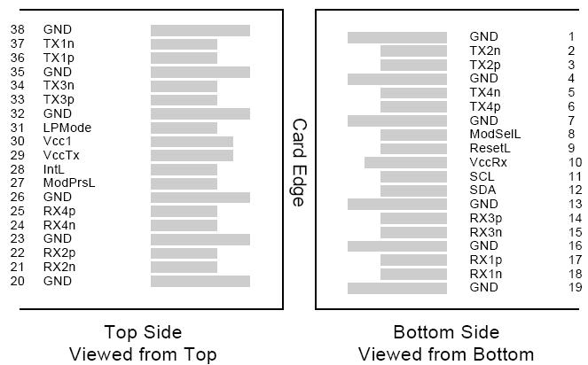
Pin Assignment
PIN | Symbol | Description | Notes |
1 | GND | Ground | 1 |
2 | Tx2n | Transmitter Inverted Data Input | |
3 | Tx2p | Transmitter Non-Inverted Data output | |
4 | GND | Ground | 1 |
5 | Tx4n | Transmitter Inverted Data Input | |
6 | Tx4p | Transmitter Non-Inverted Data output | |
7 | GND | Ground | 1 |
8 | ModSelL | Module Select | |
9 | ResetL | Module Reset | |
10 | VccRx | +3.3V Power Supply Receiver | 2 |
11 | SCL | 2-Wire Serial Interface Clock | |
12 | SDA | 2-Wire Serial Interface Data | |
13 | GND | Ground | |
14 | Rx3p | Receiver Non-Inverted Data Output | |
15 | Rx3n | Receiver Inverted Data Output | |
16 | GND | Ground | 1 |
17 | Rx1p | Receiver Non-Inverted Data Output | |
18 | Rx1n | Receiver Inverted Data Output | |
19 | GND | Ground | 1 |
20 | GND | Ground | 1 |
21 | Rx2n | Receiver Inverted Data Output | |
22 | Rx2p | Receiver Non-Inverted Data Output | |
23 | GND | Ground | 1 |
24 | Rx4n | Receiver Inverted Data Output | 1 |
25 | Rx4p | Receiver Non-Inverted Data Output | |
26 | GND | Ground | 1 |
27 | ModPrsL | Module Present | |
28 | IntL | Interrupt | |
29 | VccTx | +3.3V Power Supply transmitter | 2 |
30 | Vcc1 | +3.3V Power Supply | 2 |
31 | LPMode | Low Power Mode | |
32 | GND | Ground | 1 |
33 | Tx3p | Transmitter Non-Inverted Data Input | |
34 | Tx3n | Transmitter Inverted Data Output | |
35 | GND | Ground | 1 |
36 | Tx1p | Transmitter Non-Inverted Data Input | |
37 | Tx1n | Transmitter Inverted Data Output | |
38 | GND | Ground | 1 |
Notes:
- GND is the symbol for signal and supply (power) common for QSFP28 modules. All are common within the QSFP28 module and all module voltages are referenced to this potential unless otherwise noted. Connect these directly to the host board signal common ground plane.
VccRx, Vcc1 and VccTx are the receiving and transmission power suppliers and shall be applied concurrently. Recommended host board power supply filtering is shown below. Vcc Rx, Vcc1 and Vcc Tx may be internally connected within the QSFP28 transceiver module in any combination. The connector pins are each rated for a maximum current of 500mA.


