


100G 100m QSFP28 SR4 Optical Transceiver
The optical transmitter portion of the transceiver incorporates a 4-channel VCSEL (Vertical Cavity Surface Emitting Laser) array, a 4-channel input buffer and laser driver, diagnostic monitors, control and bias blocks.
Product Description
Multimode,100G,100m, MPO Connector, withDDM
Product Features
Applications
General Description
WTQ28-85SR4-M1B are designed for use in 100 Gigabit per second links over multimode fiber. They are compliant with the QSFP28 MSA and IEEE 802.3bm
The optical transmitter portion of the transceiver incorporates a 4-channel VCSEL (Vertical Cavity Surface Emitting Laser) array, a 4-channel input buffer and laser driver, diagnostic monitors, control and bias blocks. For module control, the control interface incorporates a Two Wire Serial interface of clock and data signals. Diagnostic monitors for VCSEL bias, module temperature, transmitted optical power,received optical power and supply voltage are implemented and results are available through the TWS interface. Alarm and warning thresholds are established for the monitored attributes. Flags are set and interrupts generated when the attributes are outside the thresholds. Flags are also set and interrupts generated for loss of input signal (LOS) and transmitter fault conditions. All flags are latched and will remain set even if the condition initiating the latch clears and operation resumes. All interrupts can be masked and flags are reset by reading the appropriate flag register. The optical output will squelch for loss of input signal unless squelch is disabled. Fault detection or channel deactivation through the TWS interface will disable the channel. Status, alarm/warning and fault information are available via the TWS interface.
The optical receiver portion of the transceiver incorporates a 4-channel PIN photodiode array, a 4-channel TIA array, a 4 channel output buffer, diagnostic monitors, and control and bias blocks. Diagnostic monitors for optical input power are implemented and results are available through the TWS interface. Alarm and warning thresholds are established for the monitored attributes. Flags are set and interrupts generated when the attributes are outside the thresholds. Flags are also set and interrupts generated for loss of optical input signal (LOS). All flags are latched and will remain set even if the condition initiating the flag clears and operation resumes. All interrupts can be masked and flags are reset upon reading the appropriate flag register. The electrical output will squelch for loss of input signal (unless squelch is disabled) and channel de-activation through TWS interface. Status and alarm/warning information are available via the TWS interface.
Absolute Maximum Ratings
Parameter | Symbol | Min | Max | Unit | Notes |
Storage Temperature | TS | -40 | 85 | °C | |
Relative Humidity | RH | 5 | 95 | % | |
Power Supply Voltage | VCC | -0.3 | 3.6 | V | |
Signal Input Voltage | Vcc-0.3 | Vcc+0.3 | V |
Recommended Operating Conditions
Parameter | Symbol | Min | Typical | Max | Unit | Notes |
Case Operating Temperature | Tcase | 0 | 70 | ºC | Without air flow | |
Power Supply Voltage | VCC | 3.14 | 3.3 | 3.46 | V | |
Data Rate, each Lane | BR | 25.78125 | Gb/s | Each channel | ||
Power Supply Current | ICC | 600 | mA | |||
Bit Error Ratio | BER | 5*10-5 | ||||
Transmission Distance | TD | 70 | m | OM3 MMF | ||
Transmission Distance | TD | 100 | m | OM4 MMF |
Electrical Characteristics
Parameter | Symbol | Min | Typical | Max | Unit | note |
Supply Voltage | Vcc | 3.14 | 3.3 | 3.46 | V | |
Supply Current | Icc | 600 | mA | |||
Module Power | P | 2 | W | |||
Transmitter | ||||||
Input differential impedance | Rin | 80 | 100 | 120 | Ω | 1 |
Differential data input swing | Vin,pp | 180 | 1000 | mV | ||
Single ended input voltage tolerance | VD | Vcc–1.3 | Vcc | V | ||
Transmit Enable Voltage | VinT | -0.3 | 4 | V | ||
Receiver | ||||||
Differential data output swing | Vout,pp | 300 | 850 | mV | 2 | |
Single-ended output voltage | -0.3 | 4 | V | |||
Notes:
- Connected directly to TX data input pins. AC coupled thereafter.
- Into 100Ω ohms differential termination.
Optical Characteristics
Parameter | Symbol | Min | Typical | Max | Unit | Notes |
Transmitter | ||||||
Signaling Speed per Lan | 25.78125 ±100 ppm | GBd | ||||
Center Wavelength | λ0 | 840 | 850 | 860 | nm | |
Average Launch Power each lane | -8.4 | 2.4 | dBm | |||
Spectral Width (RMS) | σ | 0.6 | nm | |||
Optical Extinction Ratio | ER | 2 | dB | |||
Optical Power OMA, each Lane | POMA | -6.4 | 3 | dBm | ||
Optical Return Loss Tolerance | ORL | 12 | dBm | |||
Output Eye Mask | Compliant with IEEE 802.3bm | |||||
Receiver | ||||||
Signaling Speed per Lan | 25.78125 ±100 ppm | GBd | ||||
Center Wavelength | λ0 | 840 | 850 | 860 | nm | |
Rx Sensitivity per lane | RSENS | -10.3 | dBm | 1 | ||
LOS De-Assert | LOSD | -11.5 | dBm | |||
LOS Assert | LOSA | -30 | dBm | |||
Input Saturation Power (Overload) | Psat | 2.4 | dBm | |||
Receiver Reflectance | Rr | -12 | dB | |||
Note:
1.Measured with a PRBS 2 31 -1 test pattern, @25.78Gb/s, BER<5.2*10 -5 .
Pin Assignment and Description
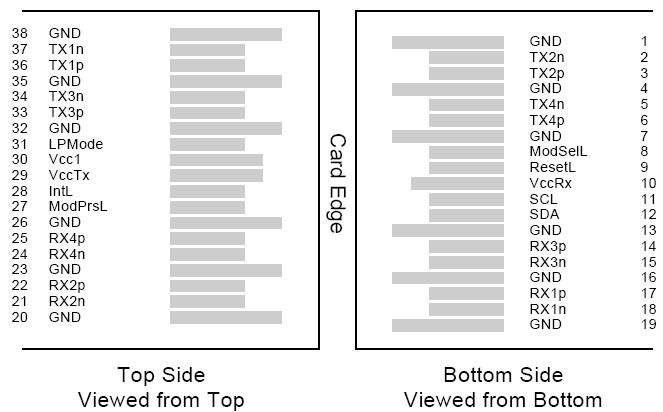
Pin Assignment
PIN | Symbol | Description | Notes |
1 | GND | Ground | 1 |
2 | Tx2n | Transmitter Inverted Data Input | |
3 | Tx2p | Transmitter Non-Inverted Data output | |
4 | GND | Ground | 1 |
5 | Tx4n | Transmitter Inverted Data Input | |
6 | Tx4p | Transmitter Non-Inverted Data output | |
7 | GND | Ground | 1 |
8 | ModSelL | Module Select | |
9 | ResetL | Module Reset | |
10 | VccRx | +3.3V Power Supply Receiver | 2 |
11 | SCL | 2-Wire Serial Interface Clock | |
12 | SDA | 2-Wire Serial Interface Data | |
13 | GND | Ground | |
14 | Rx3p | Receiver Non-Inverted Data Output | |
15 | Rx3n | Receiver Inverted Data Output | |
16 | GND | Ground | 1 |
17 | Rx1p | Receiver Non-Inverted Data Output | |
18 | Rx1n | Receiver Inverted Data Output | |
19 | GND | Ground | 1 |
20 | GND | Ground | 1 |
21 | Rx2n | Receiver Inverted Data Output | |
22 | Rx2p | Receiver Non-Inverted Data Output | |
23 | GND | Ground | 1 |
24 | Rx4n | Receiver Inverted Data Output | 1 |
25 | Rx4p | Receiver Non-Inverted Data Output | |
26 | GND | Ground | 1 |
27 | ModPrsL | Module Present | |
28 | IntL | Interrupt | |
29 | VccTx | +3.3V Power Supply transmitter | 2 |
30 | Vcc1 | +3.3V Power Supply | 2 |
31 | LPMode | Low Power Mode | |
32 | GND | Ground | 1 |
33 | Tx3p | Transmitter Non-Inverted Data Input | |
34 | Tx3n | Transmitter Inverted Data Output | |
35 | GND | Ground | 1 |
36 | Tx1p | Transmitter Non-Inverted Data Input | |
37 | Tx1n | Transmitter Inverted Data Output | |
38 | GND | Ground | 1 |
Notes:
- GND is the symbol for signal and supply (power) common for QSFP28 modules. All are common within the QSFP28 module and all module voltages are referenced to this potential unless otherwise noted. Connect these directly to the host board signal common ground plane.
- VccRx, Vcc1 and VccTx are the receiving and transmission power suppliers and shall be applied concurrently. Recommended host board power supply filtering is shown below. Vcc Rx, Vcc1 and Vcc Tx may be internally connected within the QSFP28 transceiver module in any combination. The connector pins are each rated for a maximum current of 500mA.


